 English


-
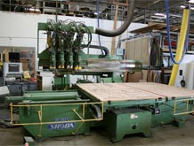
Machinery
Choose from 20,077 used machinery listings
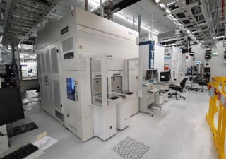
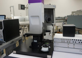
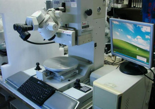
Wafer Specification
o Wafer Size: 200MM
o Wafer Shape: SNNF (Semi Notch No Flat)
o Wafer : 6”, 8” or 12”
Electron Optical System
o Electron Gun Schottky emission source (fei)
o Accelerating voltage 300V to 2000V
o Probe Current Low 5pA / Medium 10pA / High 20pA
o Electromagnetic Lens 3 Stage Electromagnetic Lens
o System with boosting voltage Beam Deflector Module
Objective Lens
o Scan Coil 2-Stage Electromagnetic Deflection (X- and Y-Axes)
o Magnification 1,000x to 400,000x (100um to 0.25um FOV)
o Wafer imaging ability Entire surface of 8” wafer
o Asspect Ratio >14 : 1
o Tilt Function 5 degrees (4 Direction)
o Resolution 3nm (500V)
SECS/GEM Communication Interface
o Automated Image Archiving Function Always / Online Setup / Never
o Measurement Function Average/Maximum/Minimum/Contact Hole/
o Line Edge Analysis/CH Analysis/Slope
o Measurement Algorithm Normal / Foot / Threshold
This equipment is located in US
| Manufacturer | Applied Materia |
| Model | VERASEM 3D |
| Year | - |
| Country |
 USA
USA
|
| Condition | Good |
| Main category | PCB and SMT equipment |
| Subcategory | Wafer & Semi Test Equipment |
| ID | P70825003 |
| Client type | Machinery dealer |
| On Kitmondo since | 2017 |
| Number of listings | 50 |
| Country |
USA
|
| Employees | 11 - 50 |
| Established | 1989 |
| Last activity | May 30, 2023 |
 Ireland
 South Korea