English
 Français
 Español
 Italiano
 Nederlands
 Português
 Ελληνικά


-
Machinery
Choose from 19,935 used machinery listings

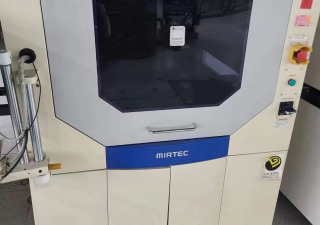
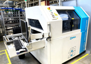
ELECTROGLAS / EG 4090u+ is a high-performance, ultra-accurate, ultra-high resolution prober used in the semiconductor industry for probing and testing semiconductor chips and die. It is capable of testing devices in a wide range of sizes and shapes with extremely high accuracy and repeatability. EG 4090 U+ includes a variety of integrated advanced features including a 3D scanner for detailed imaging and positioning of the electrodes, as well as an integrated arcing detection system for precise communications, timing and control. The advanced features of ELECTROGLAS EG4090U+ make it a superior choice for ultra-accurate testing on semiconductor wafers. It is equipped with a powerful scanning system to ensure ultra-high resolution imaging of the wafers and for accurate positioning of the probes. In addition, the automated microscope system allows for automated optical centering and alignment of the probe tip. With these advanced features, ELECTROGLAS 4090u+ probes can be accurately positioned with incredible accuracy and repeatability. This high-performance prober features a state-of-the-art communications link to the external test controller. It can communicate with a variety of test controllers for managing test sequences or directly to the tester for testing in parallel with other processes. The communication link features bi-directional mode for fast, reliable test operations and real-time data logging. This allows the prober to be integrated into comprehensive factory processes. EG EG4090U+ also includes a range of enhanced chip handling features. It is designed to quickly and accurately align and load chips onto the probes at high speed. The automated and enhanced wafer handling also makes it possible to precisely place and probe multiple devices simultaneously, even with challenging geometries. In conclusion, ELECTROGLAS / EG 4090 U+ is a high-performance, ultra-accurate, ultra-high resolution prober designed for both small and large semiconductor wafers. It offers superior optical centering and alignment, enhanced wafer handling, and powerful communications link for advanced test management and logging. All of these features make ELECTROGLAS / EG EG4090U+ an ideal choice for ultra-accurate testing on complex semiconductor wafers.
This equipment is located in SG
| Manufacturer | EG |
| Model | 4090U+ |
| Year | - |
| Country |
 Singapore
|
| Condition | Good |
| Main category | PCB and SMT equipment |
| Subcategory | PCB Inspection |
| ID | P40105006 |
| Client type | Machinery dealer |
| On Kitmondo since | 2019 |
| Number of listings | 5 |
| Country |
Singapore
|
| Last activity | Jan. 5, 2024 |
| Contact | Click here |
 USA
USA
 South Korea
 Austria
 Italy
Italy